The Integrated Main Board
The reference build is a stack of breakout modules on a carrier. That is the right way to start (every part is swappable, nothing is fatal), and it is the wrong way to finish: the wiring is fragile, the power path is whatever the cheapest TP4056 board does, and there is no ground plane. The KiCad project in hardware/pcb/ folds the whole stack onto one board that keeps the exact firmware pin map, so nothing in software changes.
This chapter is about the decisions, not the click-path. The board README has the file inventory and the current build state.
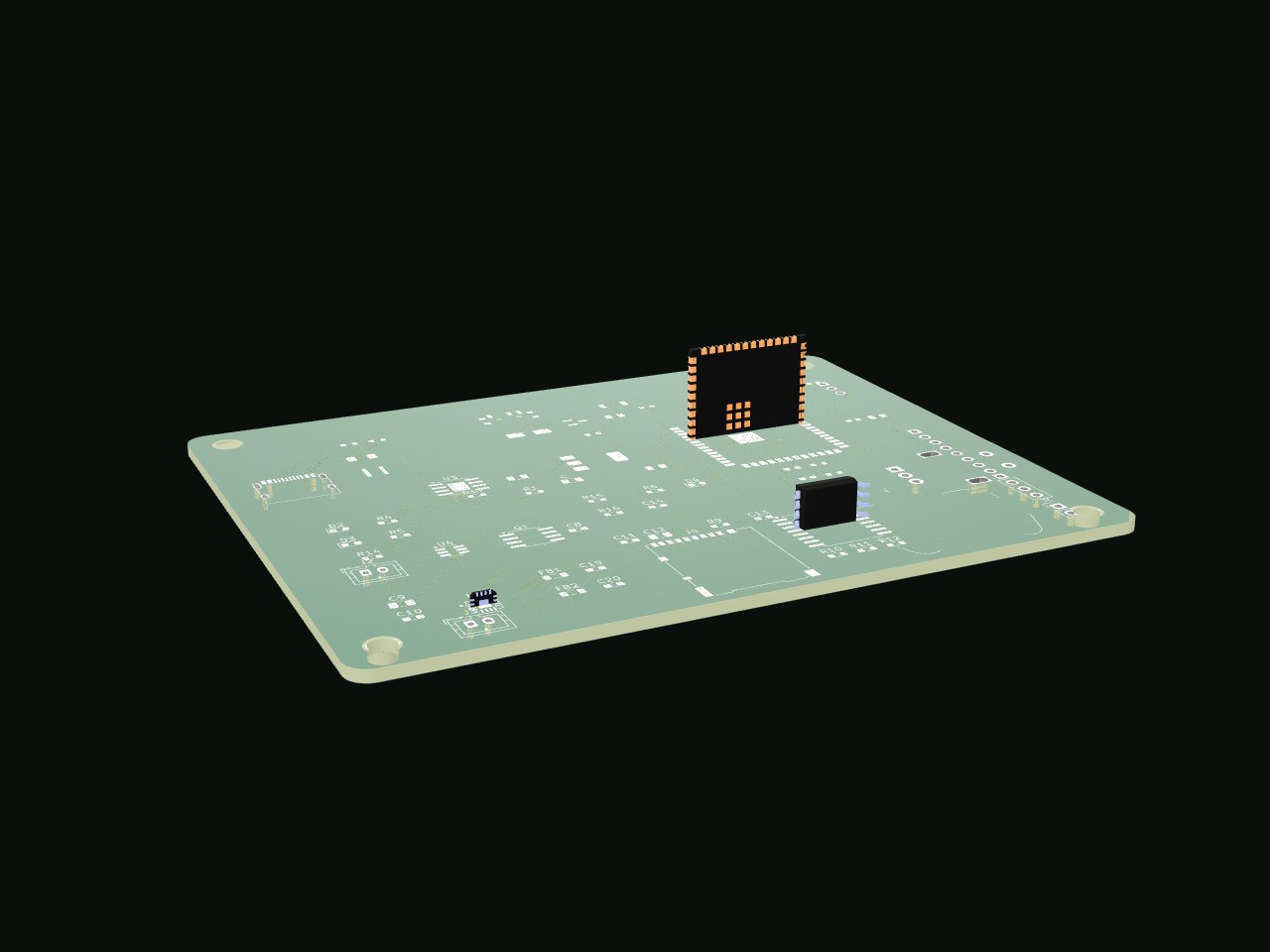
The firmware is the pin map
The single hardest constraint on a board like this is invisible: the GPIO assignment. It is defined once, in main/app_config.h, and the pinout reference is generated from it. The schematic uses those exact net names on the ESP32 pins, so the board is a physical realization of a map the firmware already trusts. Change a pin in the header, and the board must follow; the schematic never invents its own assignment. This is why the board can be reflowed and flashed with unmodified firmware.
Power: the part that earns its complexity
Everything downstream of the battery is where a Quran player that runs for years either works or slowly destroys its own cell. The chain is deliberate:
USB-C in, with real ESD. A 16-pin USB-C receptacle with the mandatory 5.1 kΩ CC pull-downs (without them a host never sources power), a PTC fuse, and a USBLC6-2SC6 TVS array on the data pair and VBUS. The ESD array sits next to the connector, because ESD protection placed after 40 mm of trace protects the trace, not the chip.
TP4056 charging, but not the bare module. The TP4056 sets charge current with one resistor (PROG) and reports state on open-drain CHRG/STDBY pins that drive two LEDs and, for CHRG, the ESP32's GPIO 17 so the firmware knows it is charging. The counterfeit two-pin TP4056 boards omit the protection IC; this design does not.
Separate cell protection. A DW01A plus an FS8205A dual-MOSFET is the standard, correct LiPo protection pair: over-charge, over-discharge, and over-current cutoff independent of the charger. The charger protects the charging process; the DW01A protects the cell from the load. Two jobs, two chips.
A load-sharing power path. This is the block people skip and regret. Without it, plugging in USB while the device runs makes the charger see both the battery and the system load, so it never terminates and the "battery full" LED never settles. The fix is an AO3401 P-channel MOSFET whose gate is pulled to VBUS: when USB is present the FET is off and a Schottky (SS34) feeds the system from VBUS while the battery charges undisturbed; when USB is absent the FET turns on and the battery feeds the system through the FET (lower drop than the diode). The system rail (VSYS) is always powered, and the battery only ever sees the charger or the load, never both.
One clean 3.3 V rail. An AP7361C LDO (1 A, fixed 3.3 V) after the power switch. A linear regulator, not a buck, because the input-to-output delta is small (VSYS is 3.3 to 5 V), the noise floor matters for the ADC battery sense and the audio, and 1 A covers the ESP32's WiFi TX peaks plus the amplifier and backlight with headroom. The battery divider (100 kΩ over 27 kΩ) hangs off VSYS into GPIO 6 with the exact ratio the firmware calibration assumes.
Why the amplifier runs at 3.3 V
The MAX98357A can take up to 5.5 V and would deliver more power there. It runs at 3.3 V on this board on purpose: its logic-high threshold scales with its supply, and at 5 V the 0.7 x VDD threshold (3.5 V) is above the ESP32's 3.3 V I2S swing, which is out of spec. Powering the amp from the same 3.3 V rail as the I2S source keeps every logic level in range, and its output through a ferrite-and-capacitor filter into the speaker is clean and more than loud enough for recitation. Correctness over a spec-sheet maximum.
The RTC shares the NFC bus
The DS3231 and the PN532 both sit on the one I2C bus (GPIO 8/9) at different addresses (0x68 and 0x24), with a single pair of pull-ups. The RTC's INT pin goes to GPIO 10 for the deep-sleep alarm wake. The coin cell holder is on the back of the board, which is both correct (it keeps the 20 mm holder off the crowded front) and a reminder that a two-layer board has two sides to place on.
Two layers, one ground plane
The board is two-layer with a ground pour on both faces. Four-layer was considered and rejected: nothing here is a controlled-impedance high-speed bus (SPI and I2C at tens of MHz, I2S audio, native USB at full-speed 12 Mbps over a short run), the WROOM module carries its own RF shield and antenna, and a solid ground pour on two layers gives a clean return path for a fraction of the cost. The engineering answer and the cheap answer are the same one here, which is the nicest kind of decision.
Manufacturing outputs
The board exports a full Gerber set with Excellon drill, a value-grouped BOM, and a pick-and-place CSV, all reproducible from kicad-cli (the commands are in the README). Component footprints target parts a fab like JLCPCB can assemble. The board is autorouted as a starting point; the README lists the short GUI pass that finishes it (the USB differential pair, a zone refill, and relieving the dense-cluster courtyard warnings), which is the honest state of any autorouted board handed to a human.
Datasheets
Every part on the board has its datasheet mirrored in the datasheet library, so a component choice can always be traced back to the source that justified it.